Currently, the problem of working a laptop in a car is quite relevant. Your laptop battery will not last long, and a car trip can last much longer than its battery life. To ensure the normal operation of the laptop from the car network, adapters are used.
There are many different adapters for working a laptop in a car. It can be purchased at a retail network, or you can make it yourself. This article is for those who are not looking for easy ways and can do something with their own hands.
There are many different schemes on the Internet. The general requirement for such an adapter is an output voltage of 18-19 volts, with a load current of about 2.5-3 amperes.
I decided to collect in this article in one heap various schemes of such adapters, the performance of which has been tested by practice. The circuits of these adapters, when properly assembled from serviceable parts, practically do not need to be adjusted and are assembled from fairly affordable parts. So, choose, as they say, to your taste and color.
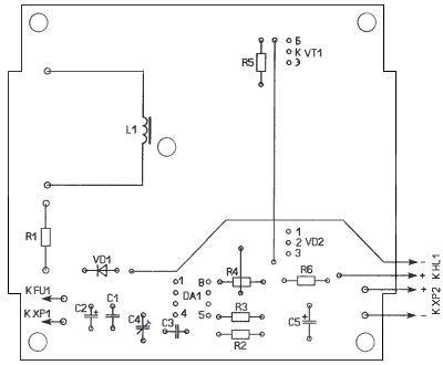
Auto-adapters for a laptop on a 555 timer.
As a PWM driver for this converter, an integrated timer KR1006VI1, an imported analogue of NE555, LM555, is used. From its output, the signal goes to a key made on a 45N03 field effect transistor, which can also be used as BUZ11, CEB603, CEP703, NDP406, IRFZ33 and many others, the main thing is that their maximum voltage is at least 40V, and the maximum current is at least 15A , well, the case is preferably TO-220.

The conversion frequency of the timer generator is determined by capacitor C1, and with the capacitance indicated in the diagram, it is approximately 40 kHz. The duty cycle of the pulses is controlled through the 5th output of the timer. Some types of imported analogues of the timer have a different control scheme for this input, and therefore may not work correctly.
As a VD2 diode, you can use a coupled Schottky diode, with a reverse voltage of at least 40V and a maximum current of at least 15A, also preferably in the TO-220 package. For example SLB1640, or STPS1545, etc. Diode VD1 - polarity reversal protection, direct current not less than 6A. Instead of VT2, KT315 is perfect. Zener diode VD3 determines the output voltage of the converter.
One of the most critical parts in this converter is the choke. It is wound on a ring of powdered iron, with a diameter of about 27 mm, used in computer power supplies as a group stabilization choke. The throttle has 21 turns, three PEV-1 wires folded together, with a diameter of 0.75 mm. Its inductance is about 44 μH and the active resistance is about 0.1 ohm.

As a housing for the adapter, a metal housing from a 50-watt electronic transformer is used. Its dimensions are 67×46×30 mm. In this case, instead of two half-bridge switches, you can conveniently place a field-effect transistor and a diode to press them against the case wall to remove heat. The transistor and diode cases must be isolated from the case with a PTFE or mica gasket.
The printed circuit board and the location of parts on the board are shown below.


The next scheme is almost the same as the first. It differs in the types of parts used in the scheme. If the exact setting of the output voltage in this circuit is not needed, then instead of PR1, VD2, R5, you can put a chain of a zener diode and a constant resistor, similar to VD3, R5 in the diagram above.
The inductor in this circuit can be wound on a ferrite ring with an outer diameter of 20 to 40 mm. with a magnetic permeability of at least 2000, and may contain 50-60 turns of wire, with a diameter of 1.0 mm. Its data is not particularly critical, it can also be wound on a segment of a ferrite rod with a diameter of 8-12 mm. and 30-50 mm long. You can also use a ready-made choke from a computer power supply.
If the voltage under load of this converter is less than necessary, then it is necessary to increase the number of turns of the applied inductor.
The following circuit is also made on an integrated timer. In terms of complexity, it practically does not differ from the above. This circuit implements protection against low input voltage of the car's on-board network, and if it drops below 9 V, the output voltage of the converter also begins to decrease, preventing throttle saturation and failure of the power switch. There is also an output protection against significant overvoltage: in the event of a feedback violation, the output voltage of the converter is limited to about 25 V.
The output voltage of this converter is 19 volts, the maximum load current is about 4.7 amperes.

The conversion frequency of this adapter can be in the range of 55...84 kHz. The voltage at pin 5 is 4.1…6 V depending on the input voltage. This range is determined by the resistance of the resistor R1. In the case of a light load, the modulating voltage may be lower than the specified values. Pin 4 of the microcircuit is connected to pin 5 so that the generator can turn off and skip pulses if necessary. Such a need occurs when the converter is operating with a small load or no load, so that a further increase in the output voltage would not occur, leading to an overload of the feedback circuit. Therefore, if the modulating voltage has dropped to about 0.7 V, a reset signal is sent to pin 4 of the microcircuit and stops the generator. Since the generator operates in stop-start mode at light load, acoustic noise may occur, but this does not interfere with the normal functioning of the converter.
Power transistor KP727B can be replaced with KP723 c letters A-B, KP746 with the letters A-B, as well as any similar imported ones, designed for a direct current of at least 15 A and having, if possible, a low open channel resistance.
The Schottky barrier diode KD272A is replaced by 2D2998 with the letters B, V, KD2998 with letters V-D, MBR1635, MBR1645, as well as any other Schottky diodes, designed for a forward current of at least 15 A and a reverse voltage of at least 25 V. The VD2 diode and the VT2 transistor must be equipped with heat sinks of 50 cm2 each.
Transistor VT1 - on any other transistors, in which the typical value of the base current transfer coefficient is about 100 at a collector current of 1 mA.
The inductor L1 is wound with a PEV-2 wire with a diameter of 1.25 mm on two annular magnetic cores KP27?15?6 made of permalloy MP140 folded together. A thinner wire connected to several cores with a total cross-sectional area of \u200b\u200babout 1 mm2 is also suitable. The winding contains 16 turns.
You can also use a yellow-white annular magnetic circuit T106-26 with dimensions of 27x14x12 mm from a multi-winding choke in the computer power supply, in this case, the winding on the choke of 24 turns of wire with a diameter of 1 mm is left, the remaining windings are removed. When self-winding, it is performed in one full layer of wire with a diameter of 1 ... 1.25 mm. Other chokes with an inductance of at least 18 μH, designed for three times the maximum load current, are also suitable.
On the other hand, the inductance of the inductor should not be too large: with its inductance of the order of 100 μH or more Feedback the stabilizer may lose stability, and there will be undamped oscillations on the collector of the transistor VT1.
To connect this device to the on-board network of a car, or similar, the wires connecting the plug and the input of the converter must have a cross section of at least 2.5 mm2. It should be borne in mind that the input current of such devices can reach 10 A. It should not flow through the spring inside the cigarette lighter plug. For this, the spring is duplicated with a wire.
Auto-adapters for a laptop on the UC3843 chip.
The adapter described below is a single-cycle switching boost converter assembled according to a typical circuit on a UC3843 chip. It provides an output voltage of 16.5 V at a current of up to 4 A.

When assembling this circuit, SMD components were used, due to which the dimensions of the assembled device are 45x30x15 mm.
The device is assembled on a double-sided printed circuit board, 37 × 23 mm in size. fiberglass, 1.5 mm thick. The top side of the board is used only as a screen and a common wire. The printed circuit board of the device (mirror image) is shown below in the figure.

Coil L1 and capacitor C9 are installed with reverse side boards (a cutout is made for the coil in the board), all other parts are as shown in the figure. The types of components used are shown in the table.

A properly assembled device does not require adjustment. If a different output voltage is required, the value of the resistor R9 should be changed, based on the fact that a voltage of 2.5 V should be obtained across the resistor R10.
Here, look at another version of this adapter using SMD elements.

Drawing of the printed circuit board of this device.
The location of the elements on the printed circuit board of this device.
The scheme of the second adapter practically does not differ from the above. The only difference is that in this circuit you can adjust the output voltage in the range of 14-27 volts. Its average load current is 2.5 amperes.
The transistors, diodes used in the circuit, as well as the data of the inductor used, are similar and can be replaced by those described in similar circuits above. Therefore, I will not dwell on this in detail.
Below in the photographs is a variant of assembling this circuit using the same SMD-= components.


If there is no need to regulate the output voltage at the output of this converter, then the variable resistor R9 can be excluded, and the resistor R8 can be selected so that the output voltage of the converter corresponds to the required one.
Auto-adapters for a laptop on the chip KR1156EU5 (MC34063).
The described device increases the voltage of the car's on-board network from 12 to 18 volts, while providing an output current of 3.2 amperes, which is quite enough to run a laptop. The device is assembled on the basis of the popular domestic chip KR1156EU5 (foreign analogue - MS34063).
A version of this converter is shown in the photo below. The printed circuit board of this converter is placed in a cast aluminum case and is closed with a lid.

Adjustment comes down to setting the conversion frequency corresponding to the maximum efficiency. To do this, the INPUT of the converter is connected through an ammeter to a DC source with a voltage of 12V and a power of at least 100 W, which can be used as a switching power supply from a computer. A load resistor with a resistance of 5.1 ohms with a power of 50W (for example, PEV-50) is connected to the output of the converter and a DC voltmeter is connected in parallel with it. Capacitor C4 smoothly changing the conversion frequency, achieve the minimum value of the output current at a constant output voltage. If it is not required to obtain the maximum efficiency of the converter, the capacitor C4 can be omitted, but the capacitance of the capacitor C3 should be 360pF.
The version of the printed circuit board and the placement of parts on it are shown in the figures below.

Another adapter, made on a similar microcircuit, differs from the above one in that its output voltage can be set within the required range using a tuning resistor, and a slightly more complicated output circuit.

This adapter is assembled on a printed circuit board, 60x35 mm in size. PCB drawing in "SL-6.0" format can be downloaded from the server.
Download PCB;
Download
Auto-adapter for a laptop on the TL494 chip.
The next auto-adapter for laptop operation from the car's on-board network is assembled from parts from computer power supplies. As a PWM controller, this adapter uses the TL494 chip, which is widely used in such power supplies, and its analogues.
The PWM controller on the TL494 chip operates here at a frequency of 40 kHz and controls the power field effect transistor.
The circuit provides with an output power of 50-60 W (at 20 V at the output) an efficiency of 90%, and with a load of 100 W - an efficiency of 85%. In this case, the output voltage ripple can reach 0.5 volts, and the maximum average input current is 12A. If such ripples are not satisfactory, then they can be reduced by increasing the capacitance of the output electrolytic capacitors.
High input current (at 100W load) requires careful PCB design. Power conductors (tracks) can be reinforced with wire. The power input cable must be at least 1.5mm2 or larger and directly soldered to the PCB.
As output power transistors, it is desirable to use those with low open channel resistance. In particular SUP75N06-07L, SUP75N03-08, SMP60N03-10L, IRL1004, IRL3705N. The BUZ11 transistor will work worse, since compared to the first one, its open channel resistance is five times greater.
You should also take seriously the choice of a power diode and a choke, which must be rated for a current of at least 10A.
Auto-adapter for a laptop on a UC1843 chip.
Another auto-adapter for working a laptop from the car's on-board network is assembled on a not very cheap and not so common microcircuit, the UC1843 PWM controller. The circuit provides an output voltage of 18 volts with a load current of up to 5 amperes. Consider the adapter circuit.
The output voltage of this adapter can be set within 16-35 volts, with a variable resistor R2. To cool the transistor and diode at a load current of up to 5 amperes, a small radiator is enough, for example, from computer power supplies. An embodiment of this circuit, see the figure below.

In this adapter, you can also use transistors and diodes, which were described in the above diagrams, since they are all basically built according to the same principle, so I will not dwell on replacing them in detail.
Auto adapters for laptops based on LT1070, LM2577T-ADJ chip.
I will give a couple more schemes of auto-adapters, using not so widespread and not very cheap microcircuits.
The first auto-adapter is assembled on the LT1070 chip. This is perhaps the most expensive and least accessible chip of all the designs described here. This is a DC-DC converter that maintains a voltage of 19 volts at the output, with a load current of 2.5-3A.
To control the output voltage level and stabilize it, the internal stabilization circuit of the LT1070 microcircuit is used. The essence of her work is that she thus changes the duty cycle of the pulses arriving at the primary winding of the transformer so that there is a constant voltage of 1.24V at pin 2 A1.
In order to obtain a stable output voltage, it is necessary from the output of the secondary rectifier to VD2, a constant voltage through the divider is applied to pin 2 A1. And the ratio of the resistors of the divider should be such that with the correct output voltage, there is a voltage of 1.24V at pin 2 A1. The divider resistors are R3 and R4.
The exact selection of R4 sets the required nominal stabilized output voltage. AT this case, it's 19V.
For winding the transformer, a ferrite ring with an outer diameter of 32 mm was taken. from ferrite 2000NM. The ring must be wrapped with a thin layer of fluoroplastic film or varnished cloth. You can not wrap the ring with anything, but cover it with a layer of epoxy pack. After it dries, you can wind the windings. It is quite possible that a ring of a different diameter and brand of ferrite can also be used to wind the transformer - you need to experiment!
The primary winding contains 40 turns of a winding wire, consisting of two PEV 0.43 wires folded together. You can use a single wire with a cross section of 0.9, but it will be more difficult to wind. The secondary winding contains 70 turns of the same double wire. First, the primary winding is wound, and then the secondary winding is wound on its surface, laying the wire in the same direction as the primary was wound. In the diagram, the beginning of the transformer windings are marked with dots.
For chokes, rings with a diameter of 18-20 mm are used. They contain 30 turns of the same double wire as for winding the transformer.
The converter circuit is assembled on a printed circuit board with a one-sided arrangement of printed tracks.
The microcircuit and diodes must be mounted on radiators. The common radiator can be a metal case in which the converter is assembled.
With proper installation and serviceable parts, the adjustment comes down to checking the output voltage. If it differs from the required one, you need to change the resistance of the resistor R4. A decrease in resistance leads to an increase in voltage, and an increase to a decrease in it.
The second adapter, similar in characteristics, is assembled on the LM2577T-ADJ chip. This circuit of all the above is probably the simplest, but the microcircuit used here is also not so widely available, although it is much more often commercially available than the LT1070 , and not as expensive as the above (seen from $ 5).
The printed circuit board for this adapter was not made, the parts were installed on a breadboard and the wiring was done with mounting wires. I will not dwell on the choice of a choke and a diode, all this is in the descriptions above, so choose to your taste.

The microcircuit is attached to an aluminum plate that serves as a heatsink, and the whole structure is placed in a suitable plastic case.
I hope that from the whole variety of the described schemes, you will find the most suitable for the execution and the most accessible radio components used in the assembly.
Good luck with the build.
For those who have to spend a lot of time on the road, and, at the same time, do not stop working, a voltage converter will be very useful, with which you can charge your laptop. This can be done in a personal car from the on-board network at 12 volts.
The DC/DC converter is great for powering your laptop while driving. This scheme is working and very functional. It provides an output current of up to 5 amps and an output voltage of 19 volts. In general, the circuit has a power of 100 watts. Part of the power is dissipated in the form of heat on some parts, such as the FET, and also on the diode assembly.
There is a diode assembly in every computer power supply. Almost each of them is designed for a voltage of 30-40 volts, sometimes the indicator reaches 60 volts. In this case, the permissible current is not less than 10 amperes. The power of the field switch affects the output current of the circuit. And in this case we are talking about IRFZ44 with a current of 49 Amps.
If desired, the key can be selected more powerful. In any case, both the field-effect transistor and the diode assembly must be on the heat sinks without fail. They get very hot, so this fact should be taken into account.
Converter features
Choke - twenty-one turns with a millimeter wire on a ring of powdered iron. Moreover, it is desirable that the wire be thicker, about one or two millimeters. To make it more convenient to wind, several strands of thin wire are wound. Both the ring and the inductor are generally taken from the power supply.

The inductor acts as a current storage, and therefore the RF bursts from the inductor are rectified using a diode assembly. After that, they accumulate in the output capacitor. This capacitor usually has a capacity of 1000-4700 uF, while the voltage is between 25 volts.

The 555 timer is connected as a pulse generator and is tuned to a frequency of about 110 kHz. In this circuit, the most effective timer frequency would be 80-150kHz. The low power transistor BC337 is successfully replaced by another low power version with reverse conduction: S9014/9018, BC556/557, KT3102/315.

The output voltage is stabilized and depends largely on the value of the zener diode, which is activated. If the required rating is not available, then zener diodes connected in series can be used. In such a situation, it is desirable that the zener diodes have a power of 1-1.5 watts, although low-power options can also work productively.

A fuse is placed at the power input, which, however, is optional. It saves the circuit from overload and unplanned short circuits at the output that can happen.
In the end, the finished converter can be installed in a small plastic case from some kind of adapter, you can even use the case from a non-working laptop charger.
When using small-sized heat sinks for a field switch and a diode assembly, it is advisable to supplement the circuit with a small cooler to remove warm air. I strongly advise you to use a metal, and even better, an aluminum case, which will simultaneously act as a heat sink for power elements.

The output power (output current) of the circuit largely depends on the field switch and the inductor, with this in mind, this inverter is capable of delivering a fairly large output current.
The efficiency of the device is at a high level, thanks to the pulse circuitry.
Using our circuit, you can build a universal voltage boost converter, i.e. get literally any output voltage (within reason). To do this, you will need to wind the appropriate inductor, replace the output capacitor and adjust the stabilization unit to the output voltage you need.
The adapter described below is a single-cycle switching boost converter assembled according to a typical circuit on a UC3843 chip. It provides an output voltage of 16.5 V at a current of up to 4 A. When assembling this circuit, SMD components were used, due to which the dimensions of the assembled device are 45x30x15 mm.
The device is assembled on a double-sided printed circuit board, 37 by 23 mm in size. fiberglass, 1.5 mm thick. The top side of the board is used only as a screen and a common wire. The printed circuit board of the device (mirror image) is shown below in the figure.

Coil L1 and capacitor C9 are installed on the reverse side of the board (a cutout is made under the coil in the board), all other parts are as shown in the figure. The types of components used are shown in the table.

A properly assembled device does not require adjustment. If a different output voltage is required, the value of the resistor R9 should be changed, based on the fact that a voltage of 2.5 V should be obtained across the resistor R10.
Here, look at another version of this adapter using SMD elements.

Drawing of the printed circuit board of this device.

The location of the elements on the printed circuit board of this device.

The scheme of the second adapter practically does not differ from the above. The only difference is that in this circuit you can adjust the output voltage in the range of 14-27 volts. Its average load current is 2.5 amperes.

The transistors, diodes used in the circuit, as well as the data of the inductor used, are similar and can be replaced by those described in similar circuits above. Therefore, I will not dwell on this in detail.
Below in the photographs is a variant of assembling this circuit using the same SMD-= components.
Business people know that a computer is indispensable in business, it is needed everywhere - at home, in the office, in the country and even in the car. But of course, it is unlikely that someone will decide to drag a computer into the car, but a laptop or netbook is easy, convenient and cozy. But here's the trouble - charging is almost dead, and the on-board network of the car is not able to charge the laptop, the inverter voltage 12 volts - 18 volts is in a hurry to help. The converter has very compact dimensions and is assembled in half an hour with all the details, it is quite simple, I think even a beginner can assemble it. The scheme has been tested and recommended for repetition.
The heart of the automotive laptop converter is the 3842/3845 chip. The transistor can also be replaced by 13007, 13009 (did not try domestic ones). Ceramic capacitors marked 105 have a capacitance of 1 microfarad. The circuit is simplified to a minimum, the transistor must be attached to the heat sink. You can use a diode bridge ready-made or make it yourself, you need to pick up powerful diodes since the current reaches up to 4 amperes.

The transformer can be wound on a ferrite ring or on a transformer from a computer power supply, the primary winding is wound with 6 strands of wire with a diameter of 0.5 mm (each), consists of 5 turns, the secondary winding is wound with 4 strands of wire of the same diameter, as the primary one, it consists of only 10 turns.

The turns of the primary and secondary windings must be stretched around the ring to increase the efficiency of the converter (efficiency up to 90%). Output capacitor with a capacity of 2200 microfarads 25 volts. We select a 820 ohm resistor with a power of 1-2 watts since it can get very hot and a low-power resistor will not withstand it. On the Internet you can find many schemes for charging laptops from the car's on-board network, but as a matter of fact they use a choke, here it was decided to use a transformer instead of a choke for some reason. Firstly, it was necessary to create a converter whose step-up part is independent of the vehicle's on-board network, since this is what can cause interference that disrupts the normal operation of the converter.

Also in this converter there is an interference suppression filter, which is simply necessary here, it is made on the basis of a choke and capacitors, the choke is made on a ferrite ring and contains 10 turns of wire with a diameter of 1-1.5 mm. The finished device is placed in a suitable plastic case.
A laptop is undoubtedly a necessary device, but the problem is that its battery does not allow you to work with it offline for more than 2 - 3 hours.
Therefore, it will be logical, when moving by car, to power and recharge the laptop from the on-board network of the car. But, unfortunately, most laptops run on 19 volts, not 12 volts.
There are few options here ... The solution to this problem can be do-it-yourself car adapter for laptop in the form of a DC voltage converter (DC - DC), which raises the battery voltage from 12 to 19 volts.
To date, there are many electrical circuits of DC-DC converters, changing the ratio of the resistance of the measuring voltage divider. which it is possible to obtain various values of the output voltage, practically from zero to 50 V.
Description of the laptop adapter
This laptop car adapter can operate from 10 to 15 V, and at the output it will be able to provide 19 V at a load current of up to 2.5 amperes. The adapter also comes with an input undervoltage protection circuitry. less than 10 V and against output overload.

The duty cycle signal controller is made on a special chip UC3843 (A2). The electrical circuit of the car adapter is almost standard. The output signals go to the gate of a powerful key field effect transistor VT1. The conversion takes place at a frequency of approximately 50 kHz. Voltage pumping takes place on L1. The adapter rectifier is made on a VD5 Schottky diode. The ripples are smoothed out first by C10, after which there is a filter of 2 inductances L2 and L3 and 2 capacitors C9 and C8.
Output voltage size laptop car adapter is determined by the resistances R11-R12. They create a voltage divider, the ratio of the shoulders of which should be such that at the desired voltage. at the output, on pin 2 A2 there was a voltage of 2.5 V. With the values \u200b\u200bof the resistances R11 and R12 shown on the adapter circuit, the output voltage will be constantly at the level of 18.75 V.
Since the instances of resistors, as usual, have discrepancies in ratings, when adjusting the size of R11 (and maybe R12) it is necessary to choose such that the output voltage is 19 V. This can be done by including additional resistors of a significantly larger value in parallel with this resistance. On the printed circuit board of the laptop adapter, there are places for them. By including resistors in parallel with R11, we reduce the output voltage, and in parallel with R12, we increase the output voltage.


The coils are assembled by hand on ferrite rings. Coil L1 is made on a ferrite ring with a diameter of 23 mm. It has 60 turns of PEV 0.61 wire. Coils L2 and L3 are assembled on ferrite rings with a diameter of 16 mm. They have 120 turns of wire PEV 0.43.
Coils L1-L3 are arranged vertically. Initially, they stand on their own conclusions, and at the end of the adjustment they are attached with a sealant. All capacities must be rated for voltages over 25 V. Diodes 1N4148 can be changed to KD522. Diode 1N4007 can be changed to KD209 or removed from the circuit altogether, however, in this case, if the polarity of the input voltage connection is incorrect. the electrical circuit may burn out before the fuse FS1.